鈻?/div>
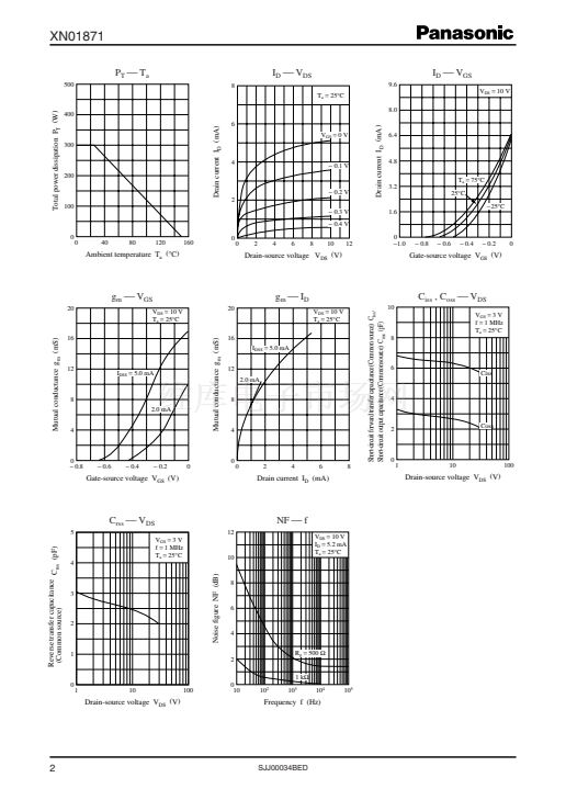
Electrical Characteristics
T
a
=
25擄C
鹵
3擄C
Parameter
Drain-source cutoff current
Gate-source cutoff current
Gate-source cutoff voltage
Mutual conductance
Short-circuit forward transfer capacitance
(Common source)
Reverse transfer capacitance
(Common source)
Noise voltage
Symbol
I
DSS
I
GSS
V
GSC
g
m
C
iss
C
rss
NV
Conditions
V
DS
=
10 V, V
GS
=
0
V
GS
= 鈭?0
V, V
DS
=
0
V
DS
=
10 V, I
D
=
10
碌A(chǔ)
V
DS
=
10 V, I
D
=
0.5 mA, f
=
1 MHz
V
DS
=
10 V, V
GS
=
0, f
=
1 kHz
V
DS
=
10 V, V
GS
=
0, f
=
1 MHz
V
DS
=
10 V, V
GS
=
0, f
=
1 MHz
V
DS
=
30 V, I
D
=
1 mA, G
V
=
80 dB
R
g
=
100 k鈩? Function
=
FLAT
Min
0.5
鈭?/div>
0.1
4
4
Typ
Max
12
鈭?00
鈭?.5
Unit
mA
nA
V
mS
12
14
3.5
60
pF
pF
mV
Note) Measuring methods are based on JAPANESE INDUSTRIAL STANDARD JIS C 7030 measuring methods for transistors.
Note) The part number in the parenthesis shows conventional part number.
Publication date: February 2004
SJJ00034BED
0.4
鹵0.2
5藲
1


 1
1
 2
2
 3
3
